| Code | ConstraintViolation |
| A – A | Acuteangle to cavity edge |
| B – B | BondPad to Bond Pad |
| B – L | BondPad to Line |
| B – S | BondPad to Shape |
| C – C | Componentto cavity edge |
| Package to package |
| Soldermask to soldermask |
| D – C | DFAPackage to package |
| D – D | MechanicalDrill Hole to Mechanical Drill Hole |
| Mechanical Drill Hole to Drill Hole |
| Drill Hole to Drill Hole |
| D – I | Negativeplane islands |
| D – L | MechanicalDrill Hole to Cline |
| Drill Hole to Cline |
| D – P | PhaseTolerance Tolerance |
| Mechanical Drill Hole to Pin |
| Drill Hole to Pin |
| D – S | MechanicalDrill Hole to Shape |
| Drill Hole to Shape |
| D – V | MechanicalDrill Hole to Via |
| Drill Hole to Via |
| E – D | MaxFinal Settle Max |
| Min First Switch Min |
| Noise Margin Min |
| Overshoot Max |
| Propagation Delay Max |
| Propagation Delay Min |
| Propagation Delay Path Type |
| Relative Propagation Delay Delta |
| Relative Propagation Delay Path Type |
| Relative Propagation Delay Scope |
| E – L | LayerSets |
| Max Exposed Length |
| Total Etch Length Max |
| Total Etch Length Min |
| E – P | Parallelism |
| E – S | MaxStub Length |
| E – T | VerifySchedule |
| E – V | MaxVia Count |
| E – X | ActiveWindow |
| Max Xtalk |
| Max Peak Xtalk |
| Sensitive Window |
| Maximum Inter Crosstalk |
| Maximum Intra Crosstalk |
| F – C | Bondfinger to component |
| Bond Pad to Component Edge |
| Bond Finger to cavity edge |
| F – F | BondPad to Bond Pad (same net) |
| Bond Pad to Bond Pad (different net) |
| I – M | Single-lineImpedance Target and Tolerance |
| J – N | AllowTs |
| K – B | BondPad to Route Keepin |
| Bond Pad to Route Keepout |
| Bond Pad to Via Keepout |
| K – C | Packageto place keepin |
| Package to place keepout |
| K – L | Lineto Route Keepin |
| Line to Route Keepout |
| K – P | ThruPin to Route Keepin |
| Thru Pin to Route Keepout |
| SMD to Route Keepin |
| SMD to Route Keepout |
| Test Pin to Route Keepin |
| Test Pin to Route Keepout |
| Test Pin to No Probe |
| K – S | Shapeto Route Keepin |
| Shape to Route Keepout |
| K – V | Viato Route Keepin |
| Via to Route Keepout |
| Via to Via Keepout |
| BB Via to Route Keepin |
| BB Via to Route Keepout |
| BB Via to Via Keepout |
| Test Via to Route Keepin |
| Test Via to Route Keepout |
| Test Via to Via Keepout |
| Test Via to No Probe |
| L – L | Lineto Line |
| L – S | Shapeto Line |
| L – W | LineWidth Max |
| Line Width Min |
| Neck Max Length |
| Neck Min Width |
| M – A | Soldermaskalignment |
| Pad Soldermask Alignment |
| Symbol Soldermask Alignment |
| M – C | SymbolSoldermask to Pad Soldermask |
| Minimum Cavity Size |
| M – L | Soldermaskto pad and cline |
| M – M | PadSoldermask to Pad Soldermask |
| Any Metal to Any Metal Spacing |
| M – P | Soldermaskto Pin |
| M – S | Soldermaskto shape |
| M – V | Soldermaskto Via |
| Matched Via count violation |
| N – S | NegativePlane to Sliver |
| O – C | Objectexposure to cavity |
| P – B | BondPad to SMD Pin |
| Bond Pad to Test Pin |
| Bond Pad to Thru Pin |
| P – D | MechanicalPin Antipad to Drill Hole |
| P – L | Lineto SMD Pin |
| Line to Test Pin |
| Line to Thru Pin |
| Mechanical Pin Antipad to Cline |
| P – M | Pastemaskpad to pastemask pad |
| Pastemask to package pastemask |
| P – P | SMDPin to SMD Pin |
| SMD Pin to Test Pin |
| Test Pin to Test Pin |
| Thru Pin to SMD Pin |
| Thru Pin to Test Pin |
| Thru Pin to Thru Pin |
| Mechanical Pin Antipad to Pin |
| P – S | Shapeto SMD Pin |
| Shape to Test Pin |
| Shape to Thru Pin |
| Mechanical Pin Antipad to Shape |
| P – V | SMDPin to BB Via |
| SMD Pin to Test Via |
| SMD Pin to Thru Via |
| Test Pin to BB Via |
| Test Pin to Test Via |
| Test Pin to Thru Via |
| Thru Pin to BB Via |
| Thru Pin to Test Via |
| Thru Pin to Thru Via |
| Mechanical Pin Antipad to Via |
| R – C | Packageto room |
| S – N | AllowEtch |
| S – S | Shapeto Shape |
| T – C | Testpointloc. to component |
| Testpoint pad to component |
| Testpoint under component |
| V – B | BondPad to BB Via |
| Bond Pad to Test Via |
| Bond Pad to Thru Via |
| V – G | AllowPad-Pad Connect |
| BB Via Stagger Max |
| BB Via Stagger Min |
| Min BB Via Gap |
| V – L | Lineto BB Via |
| Line to Test Via |
| Line to Thru Via |
| V – N | Vias |
| Vialist constraint violation |
| V – S | Shapeto BB Via |
| Shape to Test Via |
| Shape to Thru Via |
| V – V | BBVia to BB Via |
| BB Via to Test Via |
| Test Via to Test Via |
| Thru Via to BB Via |
| Thru Via to Test Via |
| Thru Via to Thru Via |
| W – A | Min.bonding wire length |
| Wire to die edge angle |
| W – D | Bondingwire diameter |
| W – C | Wireto Cavity Edge Spacing |
| Wire End to Cavity Edge Spacing |
| W – E | Wireend to wire end |
| W – F | Wireto bond finger |
| W – I | Max.bonding wire length |
| W – P | Wireto pin |
| W – W | Wireto wire (same profile) |
| W – X | Wireto wire (different profile) |
| X – D | ExternallyDetermined Violation |


 闽公网安备35062302000276号 | 闽ICP备2024076463号-1 | 论坛技术支持QQ群171867948 | 论坛问题,充值问题请联系QQ1308068381


 再发某公司的PADS格式 PCB封装库全套共享
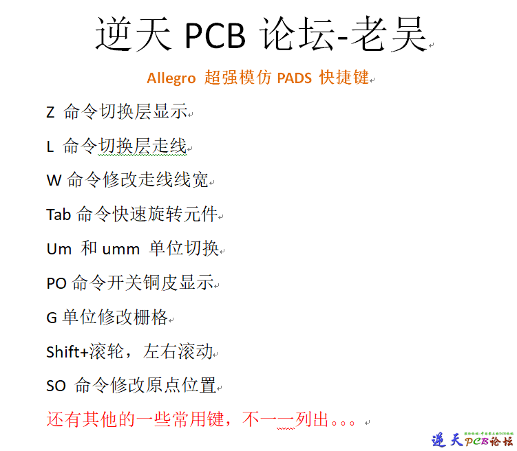 Allegro超强最全模仿PADS快捷键实现Z切换层
 双声道功放原理图PCB
 RP2040 最小系统开发板核心板PCB和原理图
 Infinity 大功率三相无刷电调无刷电机驱动
 10Gbps USB外设控制器原理图PCB
 GPS NTP Server 从GPS卫星上获取时间给局域
 allegro羊皮卷
 fpga的升压电路中的电流检测电路,使用opa2
 LED灯电阻功率,计算工具
 新手画板求助,AD9910 AD8302
 C7541613_线对板针座_ZX-MX3.0-2-2PZZ_规格
 BUCK电感,BOOST电感,BOOST滤波电容,晶振电
 佳士宝ZX7-200 直流手工焊机电路原理图共享
 MTK6228手机主板PCB及原理图AXK7L30227+TLA09ZZA
 JC-AGL-萃茶机升级版 控制板PCB文件
 RK3399核心板全套资料
 SSD SM2246EN 2.5英寸SSD的PCB原理图
 40:1匝比的平面变压器
 树莓派RP2350B 最小系统PCB和原理图
 STM32H750最小系统板,练习走线玩


 发表于 2024-1-22 12:30
 提升卡
 置顶卡
 变色卡(高亮)
 千斤顶
 照妖镜


